Intro
Main memory, or RAM, is the unsung hero behind every program your computer runs. As someone who works on enabling this vital hardware, I’m excited to pull back the curtain and explain its inner workings. This blog will dive into the hardware design of memory, revealing how RAM functions at a fundamental level and how the System-on-Chip (SoC) precisely enables it to execute programs seamlessly.
Contents
- DRAM Basics.
- DRAM Terminologies.
- DRAM Pin-outs (LPDDR4).
- DRAM signals.
- Memory Controller (MC).
- DIMM Types.
- DIMM Training.
- References
1. DRAM Basics
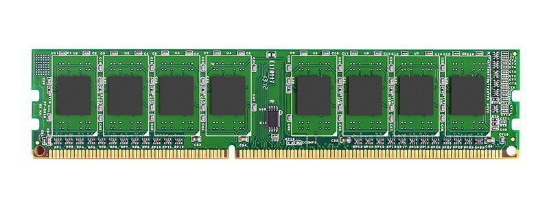
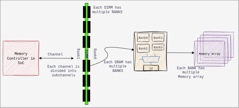
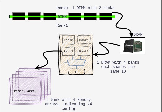
The following is how the DIMM looks like, the eight rectangular chips associated with the circuit are the DRAM chips.
The following illustrates a typical connectivity in a system:
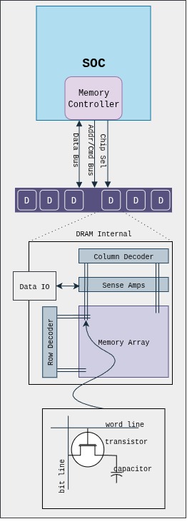
- Basic functional blocks of a DRAM: storage cells, storage array, IO structure, sense amplifiers, decoders, control logic and packaging.
- The DRAM memory array is a single transistor-capacitor pair for each bit. It is dynamic because capacitors are not perfect devices, and eventually leak; so, each capacitor must be periodically refreshed. Each DRAM die contains one or more memory arrays. Here, the transistor is turned by applying voltage on the gate then a voltage representing the data value is placed onto the bit-line and capacitor is charged. The capacitor retains the stored charge after the transistor is turned off.
- The intersection in memory array (above figure) is identified by the intersection of row and column, the memory controller (MC) accesses the stored cell in DRAM chip. The MC acts as an agent between processor and DRAM, the processors requests to the MC and it satisfies it.
- The buses connecting from MC to DRAM are JEDEC style, i.e., they are classified by their function and organisation in Data, Address, Command and Chip-select. The Address/Command bus are the same, and composed of row/column strobes, clock, etc… The chip select is responsible to select the rank.
- The Sense Amplifiers are used to detect the values stored on the capacitors. The sense amplifier detects the voltage levels in the associated bit-lines. The sense amp first precharges the bit-lines to voltage level that is halfway between logic 0 and 1 and then detected the minute changes.
Sense Amplifiers: The following are the functionality of a sense-amp:
- Sense the minute changes in voltage that occurs when transistor is turned on. The sense amp compares the voltage on bit-line vs reference voltage and then resolves to a digital value of 1 or 0.
- Restores the value of a cell after the voltage is sensed and amplified.
- Acts as a temporary data storage element. The sensed values will remain in the sense amp until another read operation takes place. Thus, sense amp ends up acting as a row buffer to cache elements.
Control Logic: the control logic is responsible for controlling the timings and sequence of signals for the sensing and movement of data, the logic accepts the external signal from MC and generates internal control signals. The modern SDRAMs have complex control logic, and with clock signal, synchronous state machines as control logic is designed. Further, programmable variability is added which allows us to control DRAM devices by using mode registers embedded as part of control logic. The synchronous natures allows pipe-lining, resulting in greater bandwidth.
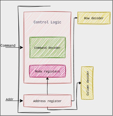
Mode Registers:
The state machines behavior is controlled using the command signals sent by MC and the programmable mode registers in the control logic. These mode registers are responsible for various control like power consumption, on-die-termination, self-test modes, write recovery, calibration modes etc.
Memory nomenclature (Parallelism can be achieved by playing with below organisation):
DRAM Size Calculation:
/* 4Gb x4 Device */
Number of Row Address bits: A0-A15 = 16 bits
Total number of rows = 2^16 = 65536
Number of Column Address bits: A0-A9 = 10 bits
Number of columns per row = 1024
Width of each column = 4 bits
Number of Bank Groups = 4
Number of Banks = 4
Total DRAM Capacity = Num.Rows x Num.Columns x Width.of.Column x Num.BankGroups x Num.Banks
Total DRAM Capacity = 65536 x 1024 x 4 x 4 x 4 = 4Gb
So, for a single DRAM chip with these specifications, the total DRAM capacity is 4 Gigabits (Gb)
/* 4Gb x8 Device */
Number of Row Address bits: A0-A14 = 15 bits
Total number of rows = 2^15 = 32768
Number of Column Address bits: A0-A9 = 10 bits
Number of columns per row = 1024
Width of each column = 8 bits
Number of Bank Groups = 4
Number of Banks = 4
Total DRAM Capacity = Num.Rows x Num.Columns x Width.of.Column x Num.BankGroups x Num.Banks
Total DRAM Capacity = 32768 x 1024 x 8 x 4 x 4 = 4Gb
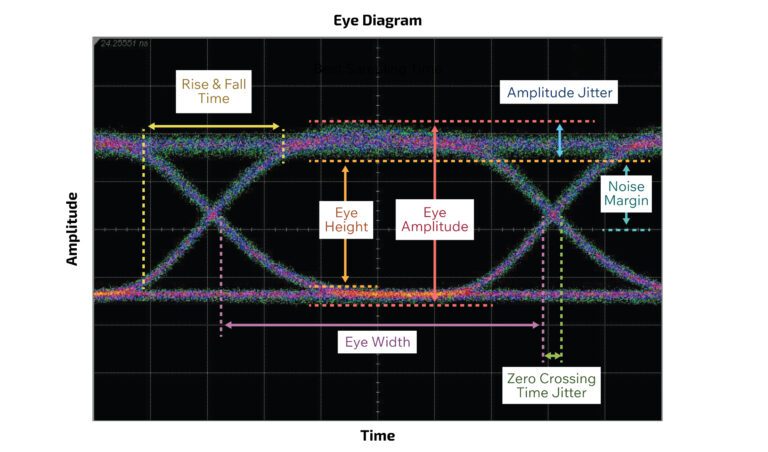
So, for a single DRAM chip with these specifications, the total DRAM capacity is 8 Gigabits (Gb)Eye diagram: it is a powerful tool used in high-speed communication to visually assess the quality of a digital signal, where a digital signal is repetitively sampled and overlaid on top of itself, triggered by the data rate or a related clock. The resulting composite waveform often resembles a human eye
Imagine a continuous stream of digital data (a series of 0s and 1s). An oscilloscope captures segments of this data stream, each segment representing a certain number of bit periods. These segments are then superimposed on the same display.
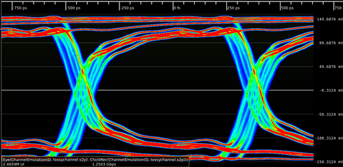
A perfect eye: (Image source: ConnectorSupplier.com)
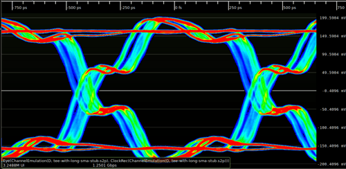
Eye with issue: (Image source: Wikipedia.org)
due to dielectric loss.
Secrets of Eye-diagram:
- Eye Opening (Vertical): This is the vertical distance between the top and bottom “rails” of the eye, indicating the voltage margin between logic 0 and logic 1.
- Large, clear opening: Good signal-to-noise ratio (SNR), sufficient amplitude to distinguish between 0s and 1s.
- Small, closed opening: Indicates noise, attenuation, or inter-symbol-interference (ISI). This can lead to a higher Bit Error Rate (BER).
- Eye Opening (Horizontal / Eye Width): This is the horizontal width of the eye at the center, representing the timing margin available for the receiver to sample the data.
- Wide opening: Low jitter, good timing margin.
- Narrow or “closed” opening: Indicates significant jitter. This reduces the time window in which the receiver can reliably sample the data.
- Rise and Fall Times: The steepness of the “slopes” of the eye diagram indicates how quickly the signal transitions between logic states.
- Steep slopes (fast rise/fall times): Good high-frequency response, allows for higher data rates.
- Shallow slopes (slow rise/fall times): Indicates bandwidth limitations or excessive capacitance, which can lead to ISI and vertical eye closure, especially for short pulse sequences (like 0-1-0 or 1-0-1).
- Jitter: The horizontal blurring or “thickness” of the transitions (the “eyelids”). Jitter is the deviation of the signal’s transitions from their ideal timing.
- Thick eyelids: High jitter.
- Thin, sharp eyelids: Low jitter.
- Noise: Vertical blurring or thickness of the “rails” (the stable 0 and 1 levels). This represents random noise superimposed on the signal.
- Overshoot/Undershoot: Spikes above the logic 1 level or below the logic 0 level, often caused by impedance mismatches and reflections in the transmission line.
- Duty Cycle Distortion (DCD): When the pulse width of a ‘1’ is not equal to the pulse width of a ‘0’. This skews the eye horizontally.
2. DRAM Terminologies
- DRAM: Dynamic Random Access memory.
- DIMM: Dual In-line Memory Module
- x4(by 4), x8(by 8), x16(by 16): the memory chip transmits or receives a number of bits equal to the number of arrays each time the MC accesses the DRAM.
- Banks: Memory arrays that operate independently of other set of memory array in a single chip. Each bank is independent of other. Memory interleaving improves performance by splitting physical memory into several banks and distributing consecutive memory addresses across them. The following diagram explains ways in which interleaving is achieved.
- JEDEC: Joint Electron Device Engineering Council (JEDEC)
3. DRAM Pinouts and function (LPDDR4)
Overview of Dual-Die, Dual-Channel, Single-Rank Package Block Diagram: (Image taken from micron LP4 spec sheet)
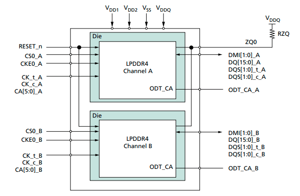
Overview of die on chip:
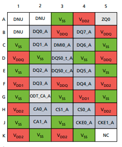
| Pin Name | Type | Description |
| CK_t_A, CK_c_A CK_t_B, CK_c_B | Input | Clock: Differential clock inputs for chA/chB. Address, command and control signals are sampled. |
| CKE0_A CKE0_B | Input | Clock Enable: Used to activate/deactivate clock. CKE is sampled at the rising edge of CK |
| CA[5:0]_A, CA[5:0]_B | Input | Command/Address Inputs: Provide the command and address inputs according to the command truth table. |
| CS0_A CS0_B | Input | Chip Select: Used to select ranks in each channel. |
| DQ[15:0]_A DQ[15:0]_B | Bidirectional | Data IO |
| DQS[1:0]_t_A, DQS[1:0]_c_A DQS[1:0]_t_B, DQS[1:0]_c_B | Bidirectional | Strobes: Differential clock signals used to strobe data during RW. The strobe is generated by DRAM for READ and by SoC for WRITE. Each byte of data has a data strobe signal pair. |
| DMI[1:0]_A DMI[1:0]_B | Bidirectional | Data Mask/Data Bus Inversion: It is used to indicate which data is masked and which is inverted in the bus. |
| ZQ0, ZQ1 | Reference | It is used to calibrate the drive strength |
| VDDQ, VDD1, VDD2 | Supply | Power supply for die |
| RESET_n | Input | Resets all channels if asserted |
4. DRAM Signals
Here we will try to understand role of above signals in read/write, which will give us basic understanding of their behavior.
- Clock (CK_t, CK_c) (heartbeat of Memory Sub-system):
- Purpose: The CLK signal (specifically, a differential pair usually denoted as CK_t and CK_c) is the master timing reference for command and address signals in the DRAM. It dictates when the DRAM samples incoming commands (like READ, WRITE, ACTIVATE, PRECHARGE) and address bits.
- The CLK signal is typically generated by the CPU’s memory controller and is distributed to all DRAM chips on the DIMM.
- Data Strobe Signal (DQS_t, DQS_c):
- Purpose: The DQS signal (also often a differential pair) is the master timing reference specifically for the DQ (data) signals. It’s a “strobe” that tells the receiver (either the memory controller during a read, or the DRAM during a write) exactly when to sample the associated data bits.
- Byte-Lane Specific: DQS is unique because it’s byte-lane specific. For every 8 bits (or sometimes 4 bits) of data (DQ[7:0]), there’s typically one associated DQS signal. This is crucial because it helps to maintain tight timing alignment between data and its clock reference, even with variations in trace lengths and signal integrity across a wide data bus.
- Bidirectional: Unlike CLK, DQS is a bidirectional signal.
- WHY DQS, when we have CLK?
- Clock Skew (Flight Time Delay): The physical path (trace length on the PCB) from the memory controller to different DRAM chips on a DIMM, or even to different data pins within the same chip, is never perfectly identical. This causes the global CLK signal to arrive at different times at different points, leading to clock skew.
- Data-to-Clock Relationship: The latency between the command (timed by CLK) and the actual data output/input (DQ) can vary slightly due to internal DRAM delays
- DQS comes in as a per-byte-lane data clock:
- Source Synchronous Timing: DQS implements a source-synchronous timing scheme for data. This means the clock (DQS) travels with the data (DQ) from the source (either the controller or the DRAM). By having DQS accompany the DQ signals on closely matched traces, any propagation delay variations due to temperature, voltage, or trace length affect both DQS and DQ almost equally.
- Eliminating Global Skew Issues for Data: Because DQS is generated and transmitted alongside its associated DQ bits, the receiver doesn’t need to rely on a distant, skewed global CLK signal for data capture. Instead, it uses the locally valid and tightly coupled DQS signal, significantly improving timing margins at high data rates.
Summary: CLK is the global reference for CA, ensuring all chips receive instructions simultaneously. And, DQS is the localized, per-byte-lane reference for data (DQ), ensuring precise timing and reliable capture of data at extremely high speeds by traveling with the data signals themselves.
So, Is DQS completely independent of CLK?
The generation and initial synchronization of DQS are still tied back to the main system CLK. DQS is not completely independent of CLK in the broader system. Both the memory controller and the DRAM internally derive and synchronize their DQS generation and reception logic to the main CLK signal. The CLK acts as the overarching timing reference for the entire memory subsystem, dictating command and address timing, and ultimately influencing the precise generation and alignment of DQS. Think of CLK as the master conductor, and DQS as a section leader who then provides precise timing to their own musicians (the DQ bits) based on the master conductor’s beat. (Gemini gives cool responses sometime)
- Data Signal (DQ[0:8]):
- Purpose: DQ refers to the actual data lines. These are the bidirectional pins on the DRAM chip (and on the DIMM) that carry the information (the 0s and 1s) being written to or read from the memory.
- Double Data Rate: As the name suggests, DQ signals transfer data on both the rising and falling edges of the associated DQS signal, effectively doubling the data rate for each DQ pin.
- DQ-DQS relationship:
- During a READ operation (DRAM to Controller): The DRAM generates DQS and sends it along with the data (DQ) to the memory controller. The DQS is edge-aligned with the DQ data. This means the DQS transitions (both rising and falling edges) occur at approximately the same time as the DQ data transitions. The memory controller uses these DQS edges to capture the incoming DQ data. Why Edge-Aligned from DRAM?: The reason is that the DRAM’s internal data paths have inherent delays. By aligning DQS edges with DQ data transitions as it leaves the DRAM, the DRAM itself can output data as quickly as possible. The burden of creating the optimal sampling window then falls to the more complex and flexible memory controller.
- During a WRITE operation (Controller to DRAM): The memory controller generates DQS and sends it along with the data (DQ) to the DRAM. In this case, the DQS is center-aligned (or phase-shifted by 90 degrees) with the DQ data. This means the DQS transitions occur in the middle of the valid DQ data eye. The DRAM uses these DQS edges to capture the incoming DQ data. Why Center-Aligned from Controller?: The memory controller has more precise control over its output timing. By carefully generating DQS to be center-aligned with DQ, it simplifies the data capture logic for the DRAM, which typically has less sophisticated timing adjustment mechanisms than the controller’s PHY.
- Command/Address Signal (CA[0:5]):
- All commands and addresses are sampled by the DRAM devices based on the edges of this CLK signal. This ensures that all DRAMs on the bus receive and interpret commands (like READ, WRITE, ACTIVATE, PRECHARGE, REFRESH) and addresses (Row Address, Column Address, Bank Address, Bank Group Address) synchronously.
- With DDR5 and LPDDR5, the CA bus has evolved to become DDR (Double Data Rate). This means that commands and addresses are sampled on both the rising and falling edges of the CLK
- Chip Select (CS):
- This control signal that tells a specific DRAM chip (or a rank of chips) whether it should “listen” to the commands and addresses currently on the CA bus by issuing an active-low signal.
- Enables CA interpretation: A DRAM will only interpret commands on the CA bus if its corresponding CS# signal is asserted. If CS# is high (inactive), the DRAM ignores the CA bus.
The DQS and CA signals are distinct and independent of each other, but they are related when we consider a certain operation like READ/WRITE/ACTIVATE etc..
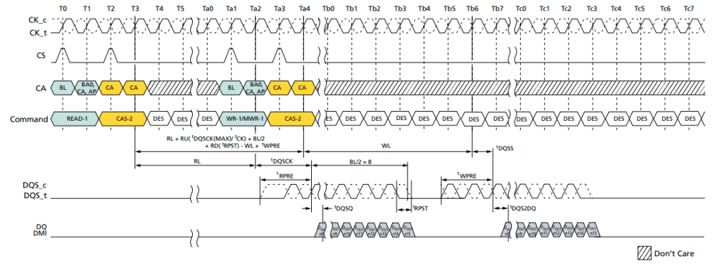
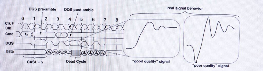
The below waveform shows everything we discussed above for READ and WRITE scenarios, it shows read followed by a write operation. Do not try to understand in detail, the below image was added just to understand how each of the above signal interact and work together execute an instruction. We will get in more detail, in further topics, as we try to understand what JEDEC talks about.
Image source: Micron LP4 datasheet.
5. Memory Controller (MC)
The MC for a given DRAM has nearly as much freedom as he design space for processor specific instruction set architecture, i.e, every other company can have different way of implementing the MC. The DRAM protocols define the interface protocol between MC and DRAM. Note, there is huge disparity in the operating frequency of modern processors and access latency to main memory.
The MC consists of two components:

- DDR controller: The controller is designed according to JEDEC standard along with the vendors own optimizations and performance capabilities. The controller connects to PHY via DFI interface to complete the solution. The controller includes command scheduler, memory protocol handler, etc…
- DDR Phy: The PHY is the direct interface to the DRAM chips. It contains the analog and mixed-signal circuitry responsible for the actual electrical signaling, including drivers, receivers, delay lines, and calibration circuits. The PHY often has dedicated hardware state machines or even a small, embedded processor to execute these training sequences. This allows it to perform the fine-grained, repetitive adjustments required without constantly burdening the main memory controller or CPU.
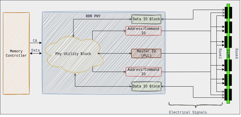
The PHY takes on much more of the “heavy lifting.” The MC hands over control to the PHY, and the PHY executes complex training sequences, generates necessary commands, and performs analysis, only reporting a “done” status and the final calibrated parameters back to the MC.
The MC and phy, these are strategies (IP owned by Synopsys, Intel, Cadence etc) unique to vendors which are used to obtain high performance and are unique.
6. DIMM Types
- UDIMM (Unbuffered DIMM / Unregistered DIMM):
- This is the most common type of RAM used in consumer desktop PCs and entry-level workstations. “Unbuffered” means that the MC communicates directly with the DRAM chips on the module.
- Pros: Lower latency, lower cost, lower power consumption.
- Cons: Due to the direct electrical load on the memory controller, UDIMM’s have limitations on how many modules and how much total capacity a system can support. This limits scalability.
- SO-DIMM (Small Outline DIMM):
- Description: A much smaller form factor, typically about half the length of a standard DIMM and less pin-counts.
- Use Cases: Laptops, notebooks, mini PCs, small form-factor embedded systems
- RDIMM (Registered DIMM):
- RDIMMs include a register (or buffer) chip on the module for the command and address (CA) and control signals. This register temporarily holds these signals for one clock cycle before sending them to the individual DRAM chips. The data (DQ) lines are still connected directly to the memory controller.
- Pros: The register reduces the electrical load on the memory controller for the CA/control lines, allowing for support of more memory modules per channel and thus higher total memory capacities. This also improves signal integrity for these critical signals. They also typically include ECC capabilities
- Cons: Slightly higher latency (due to the one-clock-cycle delay introduced by the register), higher cost, slightly higher power consumption than UDIMMs.
- LRDIMM (Load-Reduced DIMM):
- LRDIMMs take buffering a step further than RDIMMs. They include an Advanced Memory Buffer (AMB) chip that buffers all signals (command, address, control, and data – DQ).
- Pros: By presenting only a single electrical load per DIMM to the memory controller (regardless of the number of ranks on the DIMM), LRDIMMs allow for the highest possible memory capacities in a system. They significantly reduce the electrical load on the memory controller, enabling more ranks per channel. They also include ECC.
- Cons: Highest latency (due to buffering all signals), highest cost, highest power consumption among the three.
- MRDIMM (Multiplexed Rank DIMM):
- Also called MCRDIMM for Multi-Channel Registered DIMM.
- A new type of DDR5 memory module designed primarily for servers and data centers to significantly increase memory bandwidth and capacity per channel.
- MRDIMMs incorporate a high-speed multiplexer or data buffer on the DIMM. This buffer allows the memory controller to simultaneously operate two ranks (or even more in future generations) within a single DIMM module.
- Pros: Increased Bandwidth, Higher Capacity, Improved Loaded Latency.
- CUDIMM (Clocked Unbuffered DIMM):
- CUDIMM is a relatively newer type of DDR5 memory module designed for high-performance client (desktop/consumer) and workstation platforms, primarily to enable much higher frequencies than standard UDIMMs.
- The core innovation in CUDIMM is the integration of a Client Clock Driver (CKD) chip directly onto the DIMM module. The CKD acts as a re-driver or buffer for the clock signals (and potentially some control signals). It receives the clock signal from the CPU, regenerates it, and then distributes a clean, strong, and precisely timed clock signal to each of the DRAM chips on the module.
- Pros: Higher Frequencies and Overclocking, Improved Stability & Easier Overclocking.
- ECC (Error-Correcting Code) DIMM:
- Description: ECC DIMMs have an additional chip (found on all DIMMs) per rank that stores parity bits (redundant data). This allows the memory controller to not only detect but also correct single-bit memory errors on the fly, and detect multi-bit errors. They typically have 9 chips per side (e.g., 9, 18, 36 chips total) instead of the usual 8.
- Pros: Increased data integrity, system stability, and reliability. Prevents crashes and data corruption due to memory errors.
7. DIMM Training
While designing the implementation, a lot of factors are considered by the designer, like, pins which cause capacitance and inductance, signaling, signal integrity, packaging, synchronization and timings. Failing to consider these, will result in sub-optimal non-functional design.
Signal are sent from one device to another in order to communicate. The following timing diagram shows read command to 2 SDRAM devices, where data is moved from DRAM to MC as a response. A good signal is one if it transitions rapidly and settles rapidly from one signal level to another. The poor signal is anything that doesn’t show above behavior.
(Image source: Book: Memory System by Bruce Jacob, David Wang, Spencer Ng)
A basic signaling system is responsible for, where an encoded signal is sent by the transmitter along the transmission line (trace) and is delivered to receiver, the receiver must resolve the value of the signal within valid timing windows from the transmission line.
Need for training’s: Traces on PCBs,
- DIMMs are formed from multiple DRAMS mounted on PCBs. the interconnects on PCBs are mostly copper traces and vias that allow electrical signal to deliver from one point to another.
- The limitation on the speed and reliability of the data transport mechanism depends on the quality and characteristics of the traces used in the system board.
- The above limitation add certain non-idealities like attenuation, reflection, skin effect, cross talk, inter-symbol interference (ISI) and Simultaneous Switching Outputs (SSO).
- Transmission line characteristics RLC: A transmission line (like a trace on a PCB or a twisted pair) is not a simple wire. At high frequencies or over significant lengths, its properties become distributed, meaning that resistance(R), inductance (L), capacitance (C), and conductance (G) are spread along its entire length, rather than being concentrated at specific points
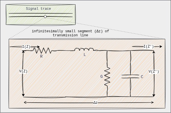
- Let us understand the above model in detail:
- Resistance (R):
- Series resistive loss in the conductors (wires or traces) of the transmission line.
- At higher frequencies, current tends to flow only on the surface of the conductor (the “skin effect”).
- Causes attenuation (signal loss) along the line, converting electrical energy into heat.
- Inductance (L):
- Series inductive property of the transmission line. It accounts for the magnetic field energy stored around the conductors as current flows.
- L is relatively constant with frequency up to very high frequencies, as the magnetic field distribution doesn’t change significantly.
- Along with capacitance, L primarily determines the characteristic impedance (Z0) and propagation velocity of the signal. Inductance causes a voltage drop.
- Capacitance (C):
- Shunt capacitive property between the conductors of the transmission line. It accounts for the electric field energy stored in the dielectric material separating the conductors.
- Mainly determined by the geometry of the conductors and the permittivity of the dielectric material.
- Similar behavior as L.
- Conductance (G):
- Shunt conductive loss or leakage current through the dielectric material separating the conductors. It’s often referred to as dielectric loss.
- G can be frequency-dependent, especially due to dielectric relaxation losses. As frequency increases, the dielectric material absorbs more energy from the oscillating electric field, contributing to loss.
- Causes attenuation (signal loss) along the line, dissipating energy in the dielectric.
- Resistance (R):
When RLCG come together as one, then:
- Skin Effect: It is a major cause of signal attenuation. The electric current doesn’t flow uniformly throughout the conductor at high frequencies, instead, the flow is limited to a certain depth of the conductor cross section when the signal is switching rapidly.
- Dielectric Loss: The dielectric material between the conductors is an insulators and electrons that orbit the atoms in the dielectric material are locked in place in the insulating material. When there is difference in potential between two conductors, the excessive negative charge on one conductor repels electrons on the dielectric toward the positive conductor and disturbs the orbits of the electrons in the dielectric material. A change in energy results in attenuating the voltage signal.
- EMI and Cross-talk: The movement of a signal in one direction involves the displacement of electrons in the other direction. A given signal and its current return path from a basic current loop where the magnitude of the current flow in the loop and the area of the loop(the return current path is generally from adjacent path or ground plane) determines the magnitude of the EMI.
Noise added into to a given trace by signaling activity from the adjacent traces are collectively referred to as cross-talk. The closely routed signal traces can attack the signal traces and impact timing and signal integrity. - Transmission Line Discontinuities / Improper termination: The trace consist of multiple segments with different characteristic impedance for each segment, signals propagating on the transmission line will be altered at the interface of each discontinuous segment.
- Multi-Drop Bus: It is used to carry cmd, addr and data signals from the MC to multiple DRAMS. When a single wire is connected to multiple devices, the propagated signal will partly reflect and gets transmitted across each impedance discontinuity, this will result in more ringing, longer delay and slower rise time. A similar behavior is observed in multiple memory socket configuration.
- Skew: A skew is introduced when the trace length between two devices of same signal is different. This happens due to poorly designed board. Skew minimization is an absolute must for high data rate signals. This is generally achieved by by design engineers purposefully adding extra twists and turns to signal paths to minimize skew between signal traces of a parallel bus.
- Jitter: It is defined as unwanted variations in amplitude or timing between successive pulses on a given signal line. To ensure the correctness of operation, signaling systems account for variations introduced into system by both skew and jitter. Jitter is difficult to deal with, generally, cuz, of the uncertainty for the cause of it.
- Inter-Symbol interference (ISI): Consecutive signals on the same transmission line can have collective, residual effects that can interfere with the transmission of subsequent signals. the interference is referred to as ISI. ISI is a band-pass filter issue. The interconnect is a non-linear low pass filter. The energy of the driver signal resides mostly within the third harmonic frequency. But the interconnect low-pass filter is non-linear, which causes the dispersion of the signal.
Summary: RLCG form the distributed model of a transmission line, defining how signals propagate and how they are affected by the physical properties of the conductor and dielectric. Their frequency-dependent behavior is critical in high-speed digital design, influencing everything from signal attenuation and distortion to characteristic impedance and reflection control.
Timing Synchronization:
Memory Training is a complex process where the CPU and Memory sub-system “train” (calibrate) the timing and electrical characteristics of the DRAM interface. This is crucial due to variations in manufacturing, temperature, and signal integrity across different memory modules and motherboards.
The whole idea of training the memory is to make sure that the signals: Command, Address, Control, Data and clock in a high speed DRAM memory system all propagate on the same type of signal traces in PCBs. To ensure proper synchronization for transmission between MC and DRAM devices. Specifically, Phase-Locked Loop (PLL) or Delay-Locked Loop (DLL) circuits are used to actively compensate for signal skews. Training’s involves things like:
- DQ/DQS Training: Aligning data (DQ) and data strobe (DQS) signals.
- Read/Write Leveling: Adjusting signal strengths and timings for optimal data transfer.
- Vref Training: Calibrating voltage reference levels.
- Impedance Calibration: Matching impedance to minimize reflections.
- and much more based on MC or JEDEC spec or complexity of the system.
8. References
- Memory Systems by Bruce Jacob, David Wang, Spencer Ng
- LPDDR4 Jedec Spec
